The Quest for Ultimate Electromagnetics using Spatial Transformations (QUEST)
A
A
A
Exeter Facilities
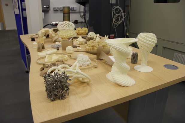
Example parts made using the facilities at CALM
Computational
Numerical and analytical modelling
We are advanced users of Ansoft HFSS and Comsol Multiphysics for finite element method (FEM) modelling of electromagnetic and acoustic systems. Differential methods for predicting the response of multilayered corrugated surfaces (diffraction gratings) have been developed, together with modal matching analytical techniques for predicting the response of well-defined photonic structures. Our team have expertise in the development of finite difference time domain (FDTD) methods for predicting the response of advanced photonic materials, including the incorporation of the Landau-Lifshitz-Gilbert equation for the study of magnetic materials.
Micromagnetic modelling of magnonic phenomena
The ability to accurately predict properties of magnetic nano-structures and devices theoretically would generate huge savings of resources, but remains elusive at present. Hence, micromagnetic modelling has become a growing area of research in Exeter. Dynamical phenomena, such as spin waves in magnetic nanostructures (magnonics) and Bose-Einstein condensation and generally kinetics of magnons, are in the focus, set by the related experimental activity. The research is currently supported through Exeter-led FP7 DYNAMAG project, which was funded by the European Commission and the DST of India to create a flexible computational framework for modelling of spin dynamics in realistic magnetic nano-materials and complete devices.
Experimental
Microwave Lab
Capability from 70kHz - 70GHz using three Vector Network Analysers (VNAs). Scalar ability up to 110 GHz. Horn antennas that can be utilised from 800-1000 MHz and 5 to 110 GHz. Microwave benches with rotating stages that provide a collimated (distance source) beam to determine the response of test samples as a function of angle of incidence. A computer controlled 3D scanner provides the ability to measure the intensity and phase of the electromagnetic fields scattered from objects under test.
High frequency electrical measurements
In addition to the VNAs described above, we also perform high frequency electrical and electro-optical measurements on both contacted devices and at the wafer level using high frequency probe stations. These experiments also utilise a 50 GHz spectrum analyzer, a 50 GHz sampling oscilloscope, a 40 GHz microwave synthesizer, and an assortment of smaller microwave frequency components. We have made measurements upon both spin transfer oscillators and phase change random access memory devices at the wafer level.
Acoustic experimentation
A collimated beam acoustic apparatus for replicating the far-field response of test samples to high frequencies. We are developing a sonar (underwater) facility. A computer controlled 3D scanner provides opportunities for mapping pressure fields.
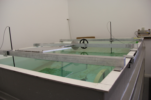 Water tank for sonar research
Fabrication
Focussed Ion Beam (FIB) and e-beam Nano-fabrication
The group has a dedicated Nova 600 system from FEI. This system is a dual-beam unit that provides the capability to undertake ion-beam milling and electron-beam lithography, as well as standard scanning electron microscopy.
Etched Nanosphere lithography (ENSL)
We have developed a fabrication methodology for producing large area patterned thin-film structures using the e-beam facility described above. The fabrication technique is based on polystyrene nanosphere self-assembly which is performed on water interface and then transferred onto thin film surfaces. The fabrication steps include reactive ion etching and thin film milling which are performed by a PlasmaPod system (JLS Design) . The system is fully automated and can operate using a combination of etching gases.
Rapid Prototyping
A Projet 3000 HD 3D-printing system that provides production of cm- and mm- sized photonic crystal and metamaterial designs for microwave experimentation with feature sizes down to 200 microns. We also have use of further college facilities in X-AT.
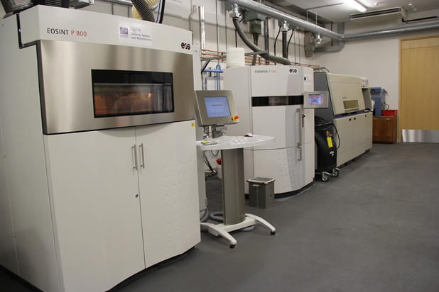
The EOS P800 and FORMIGA P100 in CALM
Deposition
Several vacuum evaporators are available for the deposition of thin metal layers which are used in the study of surface plasmons and microstructured metamaterial surfaces. We have an automated ophthalmics coater (sputterer), and associated design software, enabling optical multilayers of arbitrary design to be fabricated. Typically Si, SiO2, Zr and ZrO2 are deposited, though other materials can be used.
Rubbing machine for surface alignment
To align liquid crystals within test cells it is essential to pre-structure the glass surfaces which form the outer walls of the cells. To this end we have a bespoke surface rubbing system for rub-aligning spin coated polymer layers on glass plates.
Fabrication of nanostructured magnetic materials
Ultrathin magnetic films are deposited within a four source magnetron sputtering system with DC and RF power supplies. The system has a base pressure on the 10-10 mbar scale when sealed completely with metal gaskets while base pressures are typically on the low 10-10 mbar scale when sealed with a viton gasket for rapid changeover of substrates. An in-situ motorized mask carousel is available for fabrication of cross-strip magnetic tunnel junctions. The deposited films may be further patterned either by a nanosphere lithography technique capable of yielding mm sized domains, or by the electron beam lithography and focused ion beam facilities available within the Physics department.